Factory Tour

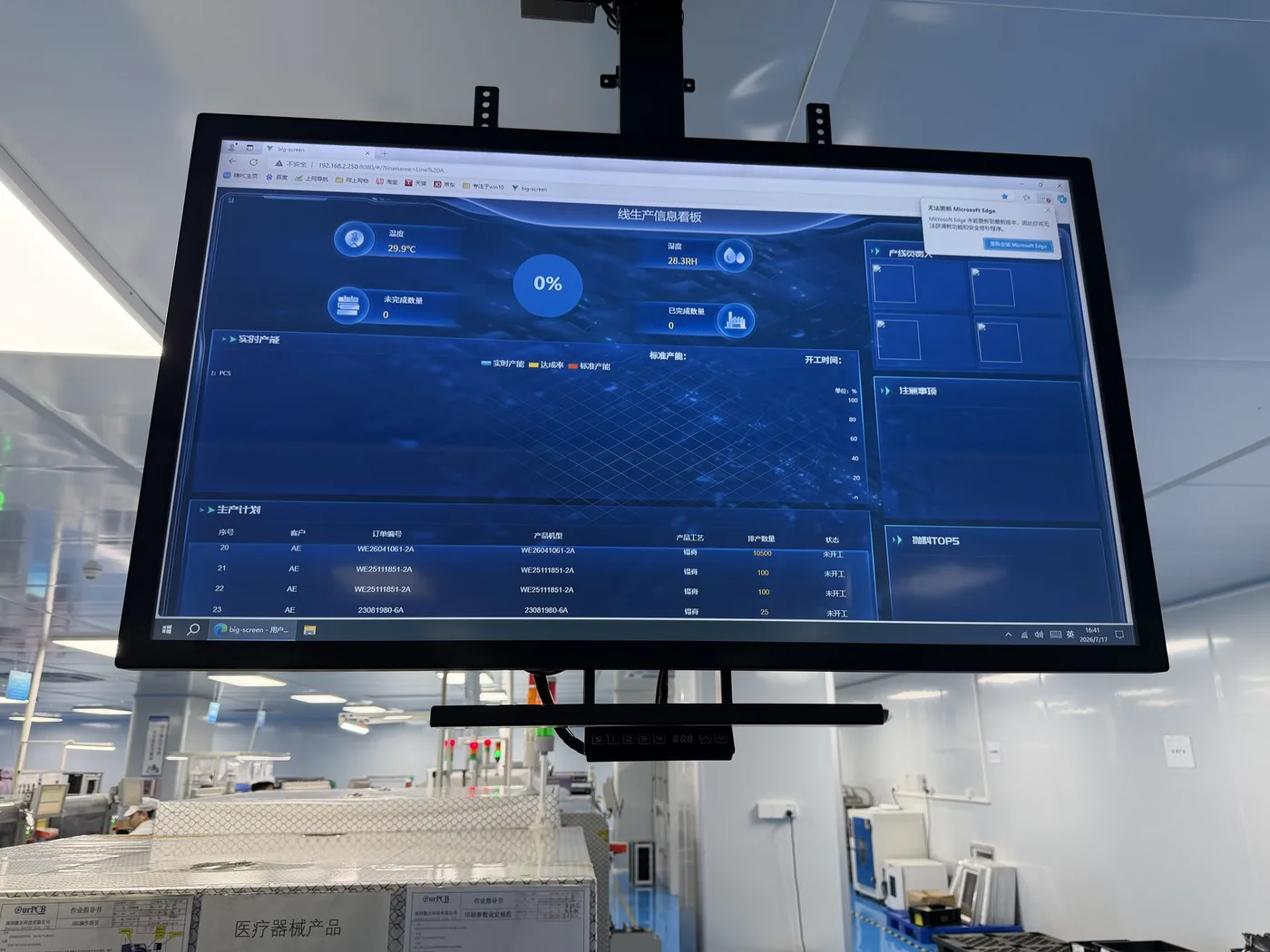
World-Class Manufacturing Facility

Explore our state-of-the-art facility equipped with the latest technology for flex and rigid-flex PCB production.

Facility Overview

Our modern manufacturing facility combines advanced automation with skilled craftsmanship to deliver exceptional flex PCB products. We maintain strict environmental controls and follow lean manufacturing principles.

12
Production Lines
10,000
Clean Room Class

Advanced Equipment

We invest in the latest manufacturing technology to ensure precision and reliability

Laser Direct Imaging (LDI)

High-precision imaging systems for fine line patterns down to 25μm trace/space.

Laser Drilling

CO2 and UV laser systems for micro-via drilling as small as 50μm diameter.

Automated Optical Inspection

Advanced AOI systems for 100% automated defect detection and quality verification.

Flying Probe Testing

High-speed electrical testing for prototype and low-volume production.

Plasma Cleaning

Surface treatment systems for optimal adhesion and reliability.

Lamination Press

Vacuum lamination systems for rigid-flex multilayer construction.

Highlights — Shenzhen SMT factory

Your flex and rigid-flex boards don't stop at fabrication. This is the in-house SMT / PCBA assembly line in Shenzhen that populates them — the equipment and controls that turn a bare circuit into a finished, tested board.
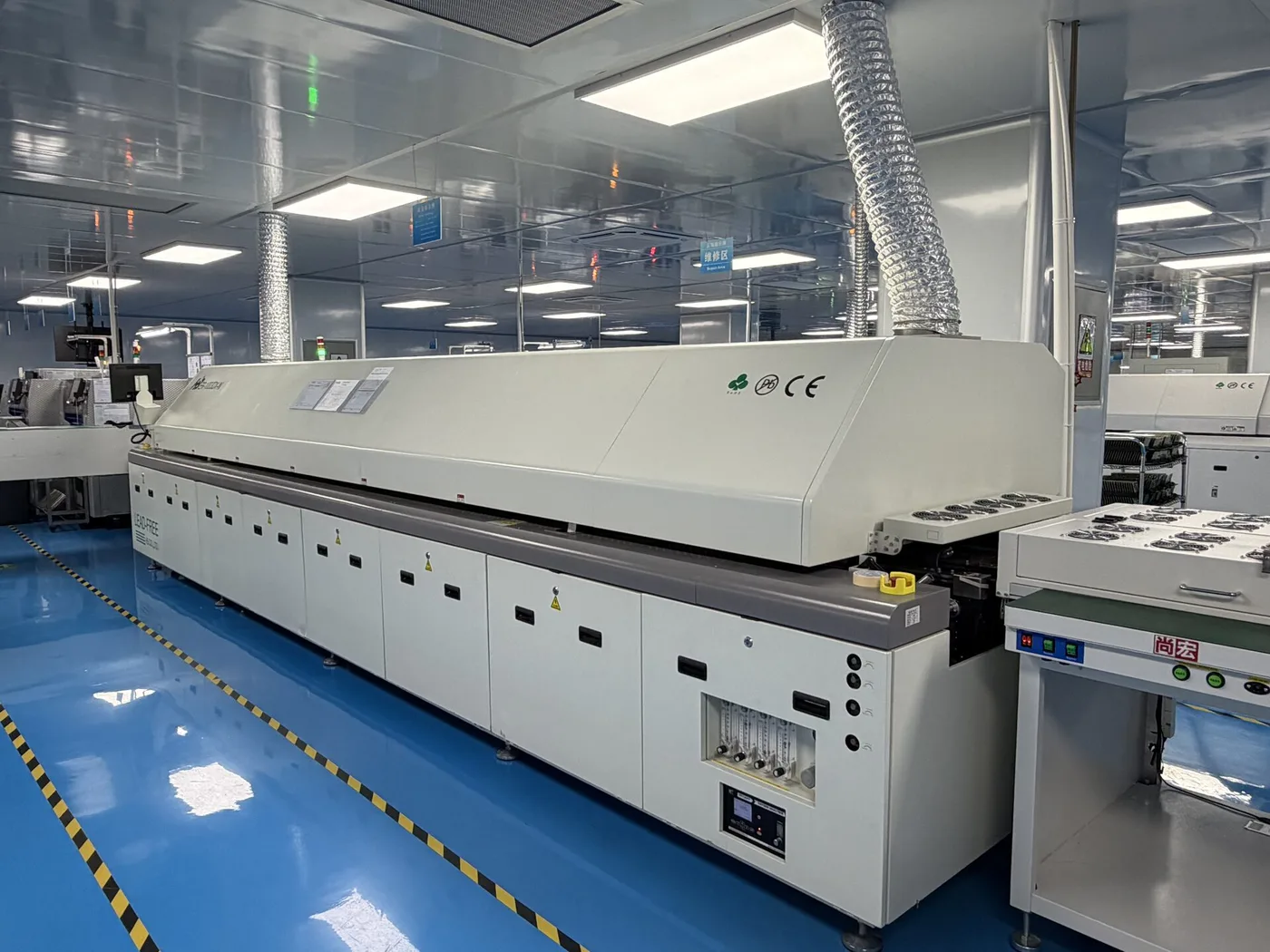
Nitrogen reflow oven on the Shenzhen SMT line
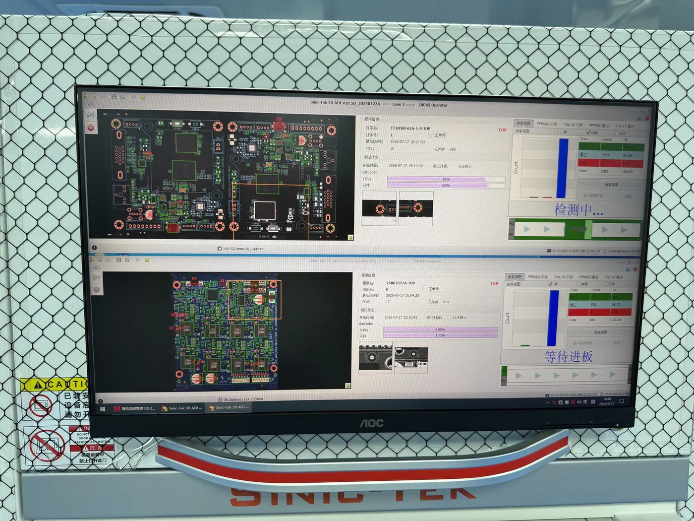
3D AOI inspection station
Per-board MES traceability scanning

4 nitrogen reflow ovens

Nitrogen reflow helps reduce oxidation-related solder defects and widens the process window for process-critical assemblies.

10 dedicated micro-feeders (4 mm tape)

Dedicated 4 mm micro-feeders give stable 01005 placement on high-density SMT builds — not something every line is set up for.

Smallest component down to 01005

01005 imperial / 0402 metric (roughly 0.4 × 0.2 mm), placed after DFM review for high-density boards.

Per-board MES traceability

Boards are serialized with unique barcodes that link their production and inspection data inside the MES.

3D SPI, AOI & selective X-Ray inspection

3D SPI and AOI depending on the assembly, with X-Ray reserved for hidden BGA and QFN joints.

Deionized-water cleaning

Assemblies are cleaned with deionized water where the process calls for it, followed by a 70× visual check for visible rosin residue.

Production Process

Our streamlined manufacturing process ensures consistent quality and on-time delivery

1

Design Review & CAM

Expert engineers review your design files and optimize for manufacturability.

2

Material Preparation

High-quality polyimide and adhesive materials are prepared in our controlled environment.

3

Inner Layer Processing

Circuit patterns are created using LDI and precision etching processes.

4

Lamination

Multiple layers are bonded using vacuum lamination for optimal adhesion.

5

Drilling & Plating

Via holes are created and plated to establish electrical connections.

6

Surface Finish & Testing

Final finishes applied and 100% electrical testing performed.

Production Process Videos

Watch our advanced manufacturing processes in action

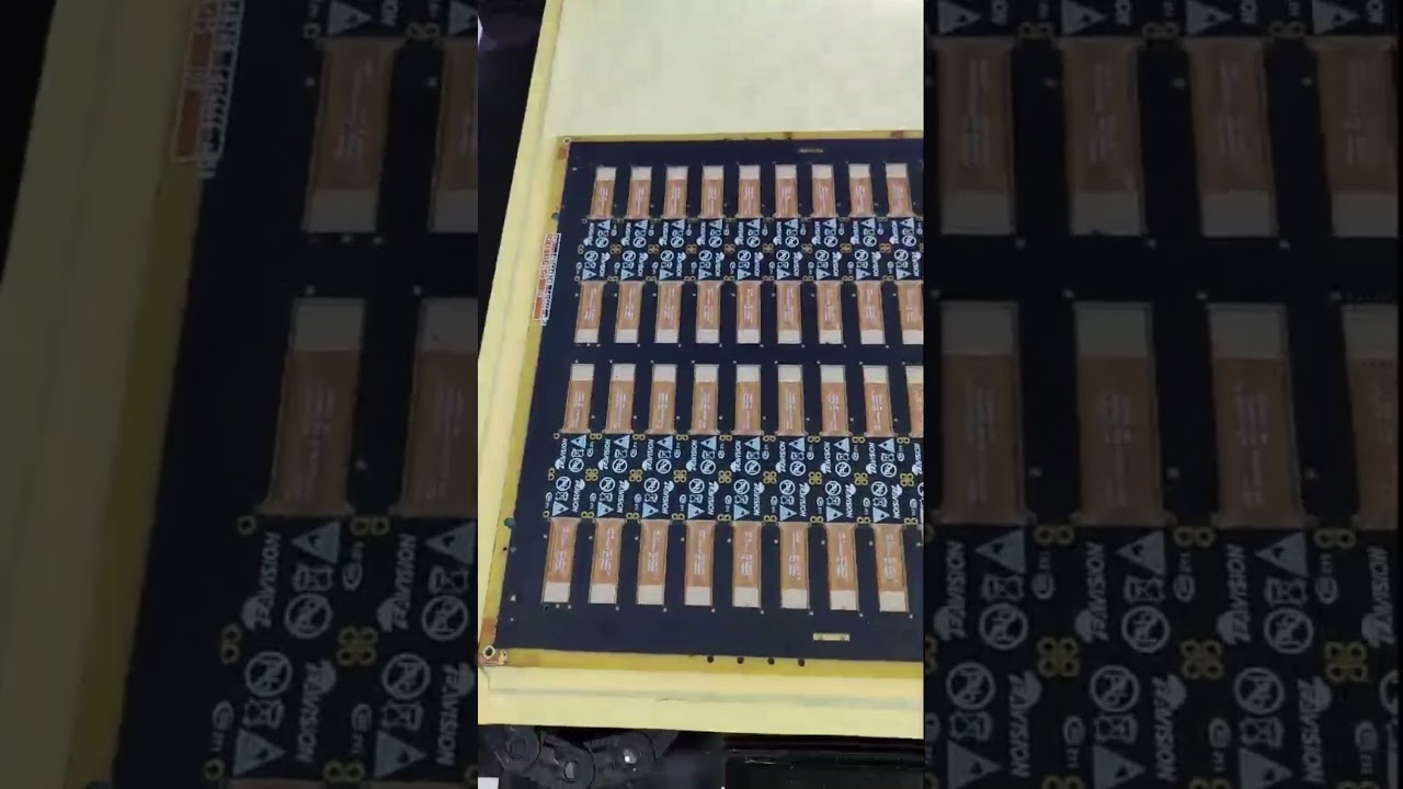
Laser Cutting Rigid-Flex PCB

Laser Cutting Rigid-Flex PCB

Precision laser cutting for rigid-flex PCB separation

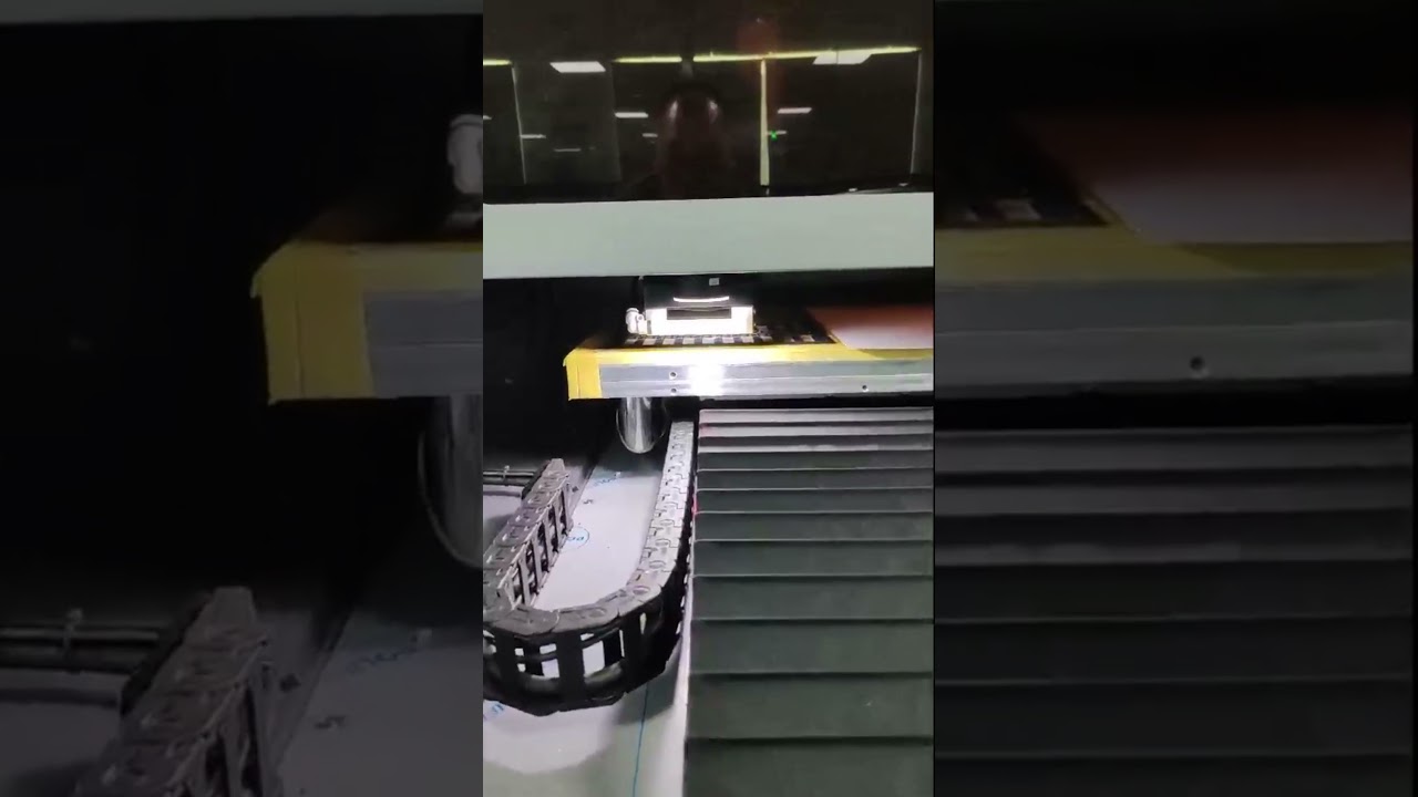
Laser Cutting Rigid-Flex PCB Part 3

Laser Cutting Rigid-Flex PCB Part 3

Advanced laser depaneling technology demonstration

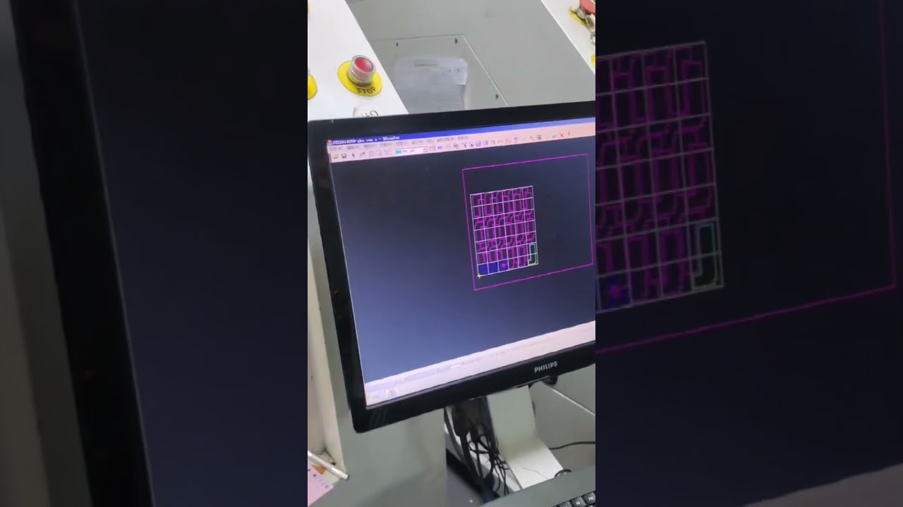
Flex Printed Board Depaneling

Flex Printed Board Depaneling

Flexible PCB depaneling process

Quality Control

Quality is built into every step of our manufacturing process. Our comprehensive QC system includes:

Incoming material inspection
In-process quality checks at each station
Automated optical inspection (AOI)
100% electrical testing
Final visual inspection
Cross-section analysis for critical orders
Reliability testing (thermal cycling, bend testing)

Ready to See Our Capabilities in Action?

Contact us to schedule a virtual factory tour or discuss your project requirements.

Contact Our Engineering Team