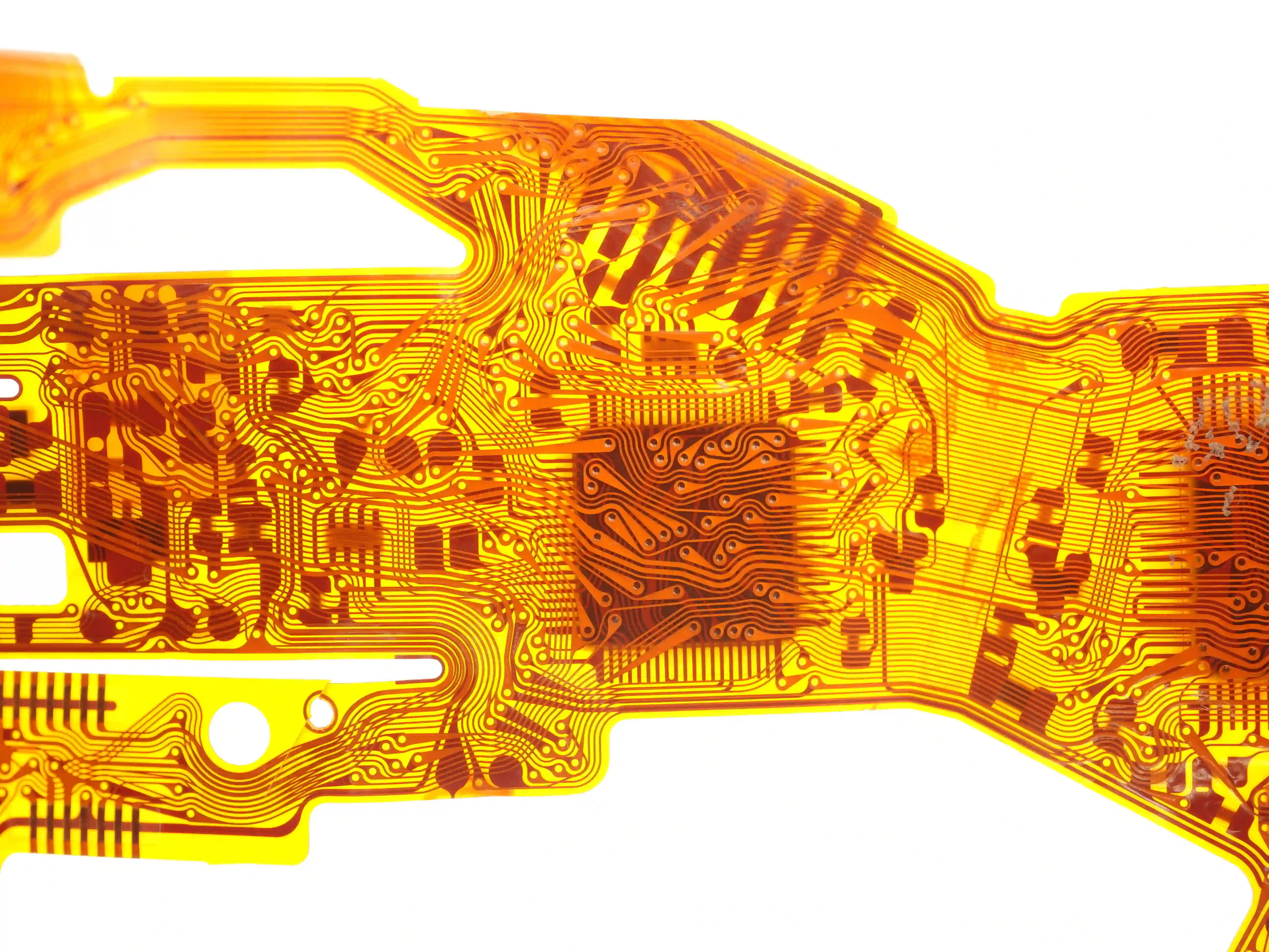
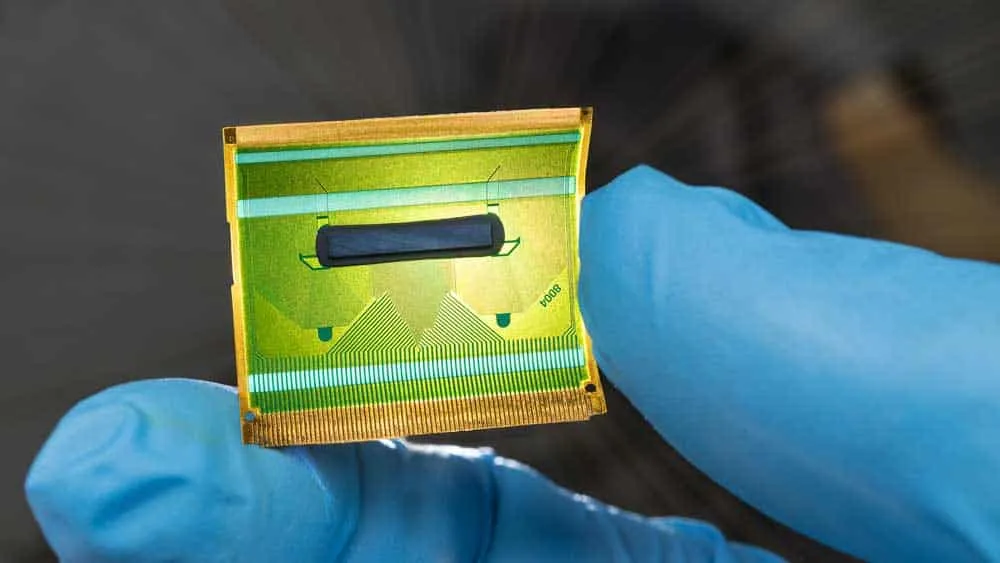
Choose EMI shielding film when a preformed shield and a compatible lamination process fit your flex stackup. Choose printed conductive silver paste or ink when selective coverage and a qualified printing/drying process fit better. Choose an etched copper layer when a defined signal return plane is central to the design. None is universally best: compare the finished construction, ground connections, bend requirements and measured electrical performance.
When comparing shielding film with conductive silver paste for flex PCB EMI control, a material's sheet resistance is only one input. It does not establish shielding effectiveness (SE) in your assembly. The comparison below covers five named products from official manufacturer documents retrieved on 2026-10-30, not every film or ink grade. Final SE must be measured on the actual stackup, with representative grounding, connectors and installed geometry.
How Film, Conductive Silver Paste and Copper Shield a Flex PCB
Shielding can reduce radiation from noisy traces and coupling into sensitive circuits. First identify the noise source, coupling path and affected circuit: a shield cannot repair every return-path discontinuity or conducted-noise problem. Camera/display interconnects, sensor tails and flex routed beside switching power circuitry are useful places to assess shielding early.
EMI shielding film: conductive adhesive plus a shielding layer
A common film construction places a metal shielding layer between an outer insulating layer and a conductive adhesive. Heat and pressure bond the adhesive to the coverlay and to exposed ground pads through designed openings. The transfer and release films used during processing are removed; they are not part of the finished stackup.
Film is a delivery format, not a single metal or construction. Some grades use deposited metal, some use thin copper foil, and others use conductive filler dispersed in resin. For example, Tatsuta's SF-PC3100-C/3300-C product sheet describes rolled copper foil, while Toyochem's LIOELM TSS series overview describes conductive filler in urethane adhesive. Select the exact grade rather than assuming all films have the same structure or flex behavior.
Printed conductive silver paste or ink: patterned coverage followed by drying or curing
A printable silver-filled material forms a conductive coating over the coverlay and connects to exposed ground lands at selected openings. The terms paste and ink describe printable formulations here; they do not mean solder paste. Printing method, deposited thickness, drying or curing conditions, substrate adhesion and any protective overcoat must be specified together.
A flexible-circuit ink is not automatically a qualified EMI shield. The Henkel grades below publish useful conductivity and processing data, but their cited datasheets do not publish shielding effectiveness. Their inclusion identifies candidates for evaluation, not approved substitutes for a shielding film.
Copper layers: an integrated shield and signal return path
An etched copper plane can provide both shielding and a signal reference when its geometry and ground connections are designed accordingly. Include the copper and associated dielectric/adhesive in the mechanical stackup. An external copper-containing film and an etched copper circuit layer are different constructions, even when both use copper.
Solid and hatched planes also behave differently. Hatching changes stiffness, return-current distribution and openings in the shield; it does not preserve a fixed percentage of solid-plane shielding. Use the hatched ground plane design guide to evaluate pattern geometry, then validate electrical and mechanical performance for your layout.
Official Datasheet Comparison: Thickness, Resistance and Shielding Effectiveness
These are manufacturer-published values, not FlexiPCB measurements or a ranking. Each source/date cell applies to every value in its row. “not stated” means the cited document does not provide that parameter. The two tables separate electrical data from processing and flex evidence so that a drying condition is not mistaken for a mechanical qualification.
Published thickness and electrical properties
| Product and official source | Thickness as published | Surface or sheet resistance as published | Published SE, frequency and method |
|---|---|---|---|
| Tatsuta SF-PC3900R1-C shielding film — product datasheet, pp. 1–2; retrieved 2026-10-30 | Total after press: 12 µm; shielding layer: 1 µm | not stated | Over 75 dB at 1 GHz and over 75 dB at 10 GHz. Reference plots: KEC E-field, KEC H-field and 7 mm coaxial-tube methods; assignment of the headline values to a method is not stated. |
| Toyochem / Artience LIOELM TSS310 film — TDS, pp. 1–2, September 2023 revision; retrieved 2026-10-30 | 10 µm after press | Surface resistance: less than 300 mΩ/□ | More than 40 dB at 1 GHz; test method: not stated |
| Toyochem / Artience LIOELM TSS500Z K2 film — TDS, pp. 1–2, August 2025 revision; retrieved 2026-10-30 | Diagram: 10 µm after press; metal layer: 2 µm. Tolerance labels are ambiguous; see note below. | Surface resistance: less than 50 mΩ/□ | More than 80 dB at 1 GHz; test method: not stated |
| Henkel LOCTITE ECI 1010 silver ink — TDS, p. 1, April 2025; retrieved 2026-10-30 | Specified finished shield thickness: not stated. Coverage calculation uses 10 µm dry coating thickness. | Sheet resistance: 0.0057 Ohm/sq/25µm, after 15 min at 120°C | SE, frequency and method: not stated |
| Henkel LOCTITE ECI 1011 E&C silver ink — TDS, p. 1, July 2026; retrieved 2026-10-30 | Specified finished shield thickness: not stated. Coverage calculation uses 10 µm dry film thickness. | Sheet resistance: 0.0029 Ohm/sq/25µm, after 10 min at 150°C | SE, frequency and method: not stated |
Thickness note: The TSS500Z K2 sheet repeats the label “Thickness of Shield layer” beside both 11 ± 4 µm and 10 ± 3 µm. Its diagram separately identifies 10 µm after press. We have not assigned those two tolerances to processing states; confirm the intended specification with the manufacturer.
Published bend tests and cure or lamination conditions
| Product and official source | Bend/flex test as published | Published processing conditions |
|---|---|---|
| Tatsuta SF-PC3900R1-C — product datasheet; retrieved 2026-10-30 | not stated | Lamination temperature, pressure, time and post-cure: not stated |
| Toyochem / Artience LIOELM TSS310 — TDS; retrieved 2026-10-30 | Quantified bend/flex test: not stated | Quick press: 150 ± 10°C, 1–3 MPa, more than 3 min; post-cure: 160 ± 10°C, more than 1 h. Alternative press-only route: 150 ± 10°C, 1–3 MPa, 30–60 min. |
| Toyochem / Artience LIOELM TSS500Z K2 — TDS; retrieved 2026-10-30 | Quantified bend/flex test: not stated | Quick press: 150–160°C, 2–3 MPa, more than 3 min; post-cure: 150–160°C, more than 1 h. Alternative press-only route: 150–160°C, 2–3 MPa, more than 60 min. |
| Henkel LOCTITE ECI 1010 — TDS; retrieved 2026-10-30 | Resistance increase after double crease test: 14%. Bend radius, repeated-cycle life and detailed fixture: not stated. | Recommended heat-drying cycle: 15 min at 120°C |
| Henkel LOCTITE ECI 1011 E&C — TDS; retrieved 2026-10-30 | not stated | Recommended drying cycle: 10 min at 150°C; technology described as heat drying and heat sintering |
Sources and Methodology
We manually compiled these five products from the linked official PDFs opened on 2026-10-30. This is a selected public-data comparison, not an exhaustive market survey or a factory test. Values retain their published limits, units and conditions; no graphs were digitized, no missing values estimated and no results converted into another test method.
Film thickness means the published after-press construction, excluding removable carriers. Ink coverage-calculation thickness is not a recommended finished shield thickness. Henkel's Ohm/sq/25µm reporting basis is retained rather than converted into a resistance at another print thickness. It is not directly comparable to a film's surface resistance without matching the measurement basis.
The Tatsuta and Toyochem sheets describe measured/internal results rather than guaranteed performance; Henkel labels its technical data as reference information. Missing SE methods prevent a controlled comparison, and the double-crease result does not establish dynamic flex life. A blank SE specification for an ink does not mean zero shielding; it means this source cannot support a numerical claim. Obtain application-specific qualification data before approving a substitution.
Decision Guide: When to Choose Film, Silver Paste or a Copper Layer
Use this table as engineering guidance, not a manufacturer capability claim. Assess the entire stackup rather than selecting the lowest resistance or thinnest individual material.
| Design priority | Film | Printed silver paste/ink | Etched copper layer |
|---|---|---|---|
| Thin shield over existing coverlay | Consider a grade with a documented after-press thickness and compatible ground openings | Control dry print thickness and include any insulating overcoat | Include copper plus any added dielectric and adhesive |
| Selective shielding around cutouts or exposed contacts | Requires cutting, registration and insulation of exposed conductive edges | Screen or other qualified printing process defines coverage; inspect edges and skips | Defined by circuit artwork and etching |
| Repeated motion | Qualify the specific film, adhesive and FPC construction at the actual bend radius | Qualify adhesion, cracking and resistance change after cycling | Qualify foil, pattern and neutral-axis placement; solid copper is not automatically unsuitable |
| Signal reference and impedance | Model conductive layer, spacing, loss and ground contact | Model the real coating and contacts if used as a reference | Often the starting point for a defined return plane; still requires stackup control |
| Process fit | Lamination pressure/temperature and possible post-cure must suit the FPC | Drying/curing, solvent compatibility and print consistency must suit the FPC | Integrated into circuit fabrication and lamination |
| Rework | Removal can damage coverlay or ground lands | Touch-up changes thickness and cure history | Plane changes generally require revised fabrication |
A film is a reasonable starting candidate for a thin tail needing broad coverage when its lamination process is already qualified. A printed coating is a reasonable candidate for patterned coverage when the supplier can control adhesion, continuity and drying on the chosen coverlay. A copper plane is a reasonable starting candidate when the design depends on a well-defined return path. These are starting points for evaluation, not universal winners.
Design Rules for EMI-Shielded Flex PCBs
Include the complete shield in thickness and bend-radius review
Count every permanent layer: base dielectric, circuit copper, adhesives, coverlay, shield, and any protective coating. Added material changes bending stiffness and the neutral-axis position; thickness alone cannot predict fatigue life. A thin film's metal or ground connection can still fail if its location and strain are unsuitable.
Separate installation folds from repeated movement. Specify the actual radius, bend angle, direction, mechanical restraint and required cycles. Keep shield edges, thickness steps and ground-contact transitions away from the highest-strain region where practical. Use the flex PCB bend-radius design guide to frame the mechanical review, then qualify the complete shielded construction. Do not transfer a generic thickness multiplier or a material coupon's cycle count to the finished part.
Ground film and paste through intentional coverlay openings
Show the ground lands and coverlay windows on the fabrication drawing. The film's conductive adhesive or printed material must reach clean, exposed ground copper without bridging to signal pads. Specify registration, opening geometry, contact area, finish compatibility and clearance to neighboring conductors with the fabricator.
Distinguish through-thickness contact resistance from in-plane sheet resistance. An anisotropic adhesive connects through its thickness; the separate shielding layer carries current laterally. A low resistance measured across a coating does not prove a reliable contact through a coverlay opening.
Ground connections have inductance as well as DC resistance. Long, narrow connections can undermine high-frequency shielding even when a continuity test passes. Choose connection locations around the actual return-current paths and connector/chassis arrangement. There is no universal ground-window pitch for all flex circuits. Keep vias and abrupt reinforcement transitions outside active bend regions where possible.
Model impedance with the shield present
A nearby conductive layer changes the electromagnetic field around a trace, whether it is called a shield or a reference plane. Film and ink therefore belong in the impedance model. They are not electrically invisible, and an absolute statement that they can never participate in an impedance-controlled construction is too broad.
Use the actual dielectric spacing, conductor geometry, coating properties and grounding arrangement. An etched copper reference plane is often easier to define; using film or ink as part of the return structure requires appropriate material data and validation. Evaluate impedance and insertion loss on the final construction, including partial-shield boundaries. Discuss the shielded stackup in the flex PCB impedance-control review, and define representative impedance coupons before fabrication.
Preserve continuity at edges, connectors and rigid-flex transitions
Shield coverage on a flat drawing does not guarantee a continuous shield in the folded assembly. Examine connector exits, slots, exposed edges, stiffener boundaries and rigid-flex steps. These can introduce gaps or concentrate mechanical strain.
Choose overlap and termination geometry for the actual construction rather than applying a universal overlap distance. Check insulation around cut film edges and printed-coating boundaries. Compare emissions or susceptibility with the flex in its installed shape, including its connection to adjacent boards and the enclosure.
Manufacturing Steps, Rework and Cost Drivers
Film lamination versus silver-paste printing
For film, the process typically includes preparing the coverlay and ground openings, cutting and aligning the film, temporary attachment, pressing, carrier removal and any specified post-cure. The Toyochem sheets above provide separate quick-press/post-cure and press-only routes. Follow the selected grade's instructions and qualify pressure distribution over steps and openings.
For printed silver, the process includes substrate preparation, material mixing, printing, drying or curing, and inspection of continuity and ground contact. Add and qualify an insulating overcoat where the assembly needs one. The Henkel drying temperatures above are product-specific starting conditions, not a generic silver-paste recipe; validate actual part temperature and substrate compatibility.
For copper layers, define the shield in the circuit artwork and stackup, including ground connections and dielectric spacing. Manufacturing and electrical inspection then cover the integrated conductor construction. Changes can affect layer count, routing and mechanical balance.
Rework must preserve the qualified construction
Do not assume that laminated film peels off cleanly or that a silver-paste patch is an equivalent repair. Removal, solvents, local heat or added coating can alter insulation, adhesion and contact resistance. Establish an approved repair process and recheck the affected electrical and mechanical requirements. An unqualified patch should not be treated as production-equivalent shielding.
Compare quotes using the same coverage and acceptance criteria
There is no defensible universal cost premium for film, silver paste or copper. Compare material utilization, covered area, number of shielded faces, tooling, print or lamination steps, added insulation, inspection and qualification scope. A cheaper raw material can require more processing. Request like-for-like quotations against the same drawing and acceptance plan rather than applying a fixed percentage to an unshielded PCB price.
How to Specify and Validate EMI Shielding When Ordering
For a flex PCB fabrication enquiry, include:
- Electrical objective: noise source, susceptible circuit, frequency range, operating modes and the required emissions or immunity margin.
- Material and construction: exact film or ink grade, shielded faces, coverage drawing, permanent layer thicknesses and proposed alternatives.
- Grounding detail: coverlay openings, ground lands, connector/chassis connections and contact-resistance acceptance criteria.
- Mechanical duty: installation fold or dynamic motion, radius, angle, restraint, cycle target and environmental exposure.
- Signal integrity: impedance targets, reference structure, transmission requirements and coupon plan.
- Process and acceptance: lamination/drying route, adhesion and insulation checks, rework limits and traceable material identification.
Validate in stages: inspect coverage and contacts, measure the agreed electrical properties, then assess shielding on representative stackups and the assembled product. Repeat relevant measurements after bending and environmental conditioning. Define pass/fail criteria before testing; a datasheet dB value cannot guarantee product-level EMC compliance. The flex PCB reliability testing guide helps organize the broader qualification plan.
FAQ
Is EMI shielding film better than conductive silver paste on flex PCB?
It depends on the finished construction. Film provides a preformed layer that must be laminated and grounded correctly. Silver paste or ink allows printed coverage but needs control of deposited thickness, adhesion and drying or curing. Compare named products and validate shielding, impedance and bending on the actual stackup; a generic material ranking is insufficient.
Does lower sheet resistance mean higher shielding effectiveness?
Lower sheet resistance can help conductive shielding, but it does not determine assembly SE by itself. Frequency, field type, openings, geometry and ground-contact impedance also matter. Compare measurements made under matching conditions. Do not calculate an ink's shielding dB from its sheet resistance alone.
Can shielding film replace a copper ground plane for controlled impedance?
It may participate in the reference structure if its conductive layer, dielectric spacing, losses and grounding are modeled and validated. It is not an automatic replacement for an etched copper plane. Include every nearby shield in the field model and verify the final construction with appropriate coupons and measurements.
Can I shield only one area of a flex PCB?
Yes, selective film or printed coverage can be designed around specific noisy or sensitive regions. Define the boundary, grounding and insulation carefully: a shield edge can change impedance, and an uncovered connector exit can remain a coupling path. Test the installed assembly rather than assuming partial coverage will meet the electrical target.
How do I qualify shielding for a flex circuit that bends repeatedly?
Test the complete construction at its intended bend radius, angle and restraint, with the required cycle count and environment. Check shield continuity, ground-contact resistance, insulation and relevant electrical performance before and after cycling. A published double-crease result or an unquantified flexibility claim does not establish dynamic service life.
Last Updated: October 30, 2026