
フレキシブルPCBメーカー
20年以上の信頼と実績
業界リーダー企業からの信頼


即時お見積り
ガーバーファイルをアップロードして、即座にDFM解析と競争力のある価格をご確認ください。
柔軟性のための エンジニアリング
当社の製造プロセスは、動的曲げからタイトな折り畳みまで、フレキシブル回路特有の幾何学的課題に対応するよう設計されています。
当社の回路が支える産業分野

医療機器
インプラント、モニター、手術ロボット向けの信頼性の高いフレキシブル回路。

航空宇宙・防衛
MIL-SPEC規格に適合した高信頼性リジッドフレックス基板。

自動車
センサー、インフォテインメント、ECU接続向けの耐久性PCB。

民生用電子機器
ウェアラブルおよびモバイルデバイス向けのコンパクトで折り畳み可能な回路。
業界アプリケーションショーケース
様々な業界向けに設計されたリジッドフレックスPCB製品をご覧ください
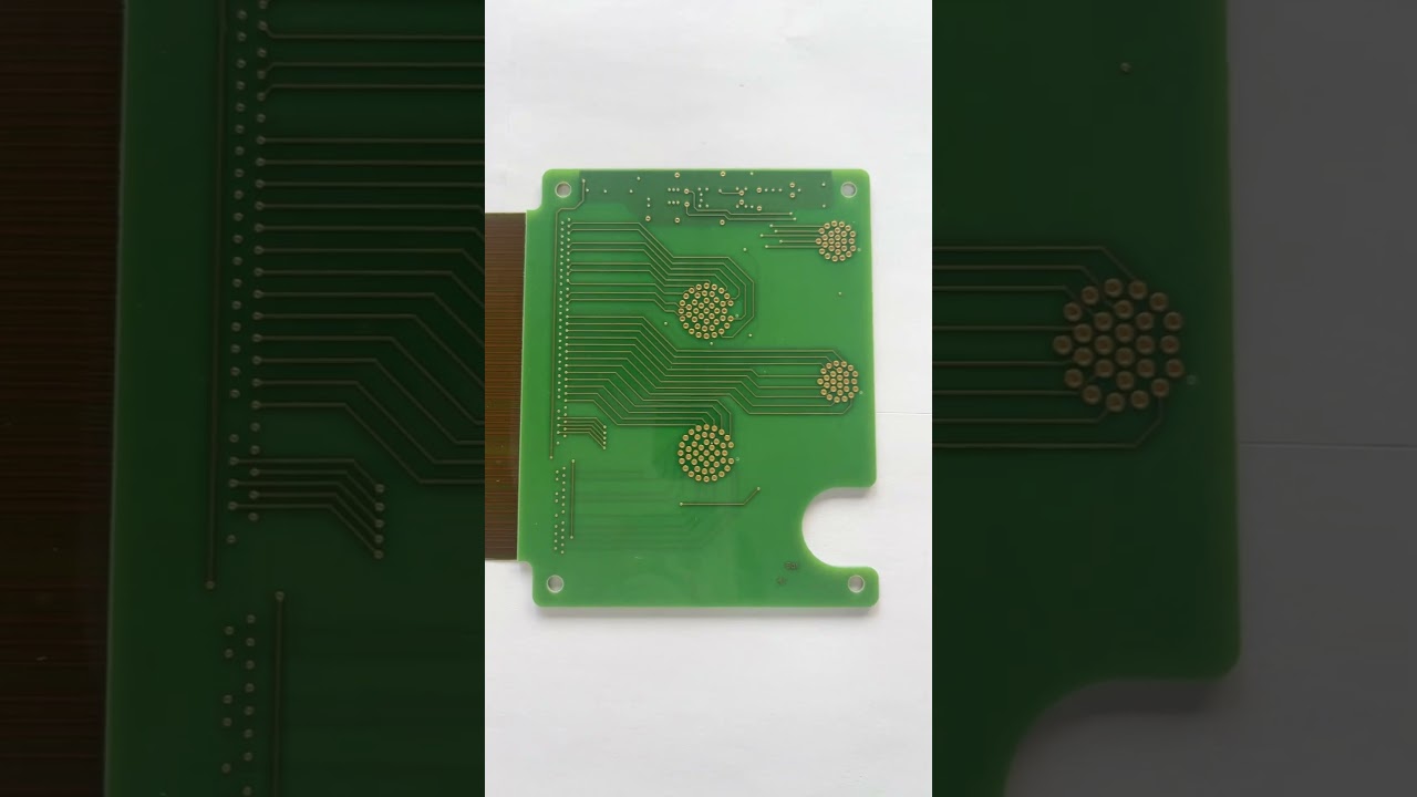
民生用電子機器向けリジッドフレックスPCB
民生用電子機器向けのコンパクトなリジッドフレックスソリューション
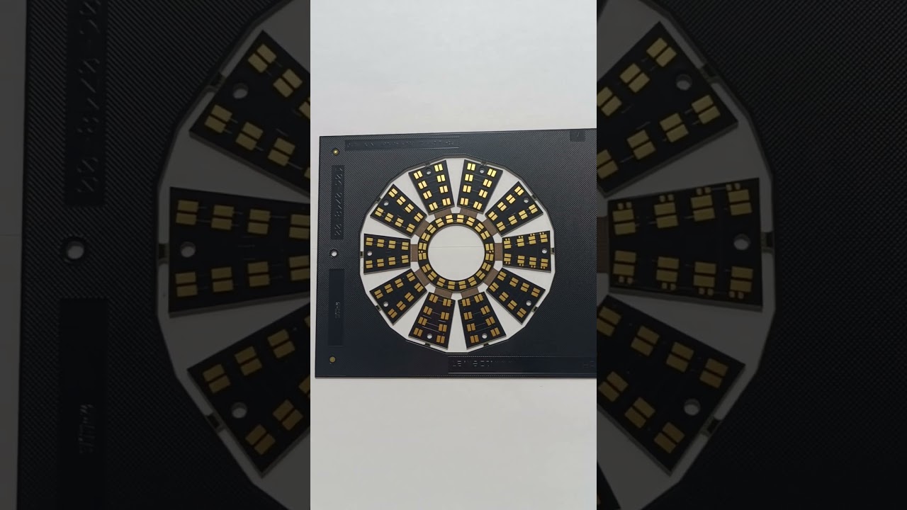
産業制御向け4層リジッドフレックス基板
産業オートメーションシステム向けの高信頼性リジッドフレックス
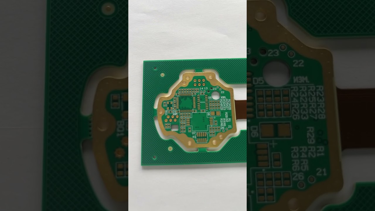
医療機器向けリジッドフレックスPCB
医療機器アプリケーション向けのカスタマイズされたリジッドフレックスソリューション
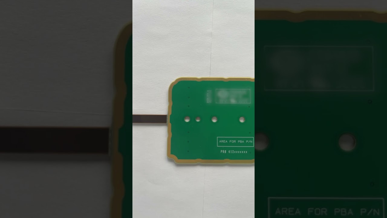
民生用電子機器向けリジッドフレックスPCB
ポータブル民生用製品向けの先進的なリジッドフレックス設計
なぜフレキシブル回路にFlexiPCBを選ぶのか?
FlexiPCBは、世界中のお客様に高品質で精密設計されたソリューションを提供する、フレキシブルプリント基板(フレックスPCB)およびリジッドフレックスPCBの大手メーカーです。当社の最先端製造施設は、先進技術と数十年の専門知識を組み合わせ、最も厳しい仕様を満たすフレキシブル回路を提供しています。
単層フレキシブル回路から複雑な多層リジッドフレックスアセンブリまで、幅広いフレックスPCBアプリケーションに対応しています。HDI技術、インピーダンス制御、ENIG、OSP、ハードゴールドメッキなど、様々な表面処理に対応しています。

ISO 9001:2015、ISO 13485(医療)、IATF 16949(自動車)認証を取得しており、すべての製品で一貫した品質を確保しています。卓越性へのコミットメントにより、医療機器、航空宇宙、自動車、民生用電子機器など、様々な業界の信頼できるパートナーとなっています。