Highlights — Shenzhen SMT factory
Your flex and rigid-flex boards don't stop at fabrication. This is the in-house SMT / PCBA assembly line in Shenzhen that populates them — the equipment and controls that turn a bare circuit into a finished, tested board.
26 placement machines across 11 SMT lines
YAMAHA YSM20R-2 high-speed and YSM10 high-precision platforms, with capacity for up to 20 million placements per day.
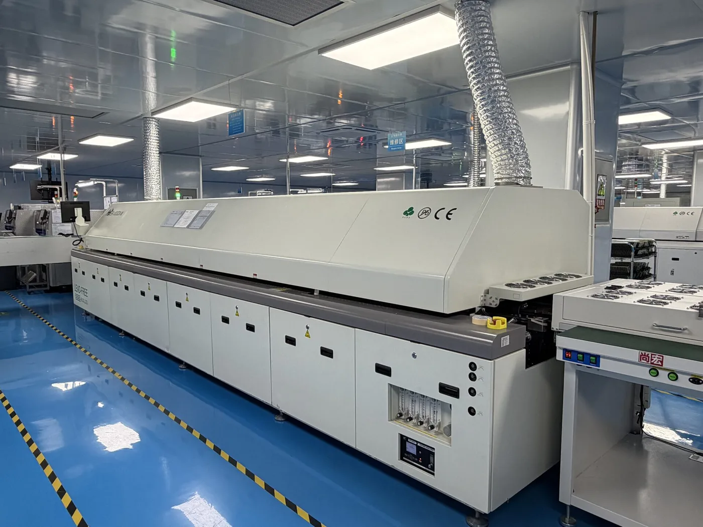
4 nitrogen reflow ovens (O₂ at 500–2,500 ppm)
Four of our six reflow ovens run a nitrogen atmosphere with oxygen controlled at 500–2,500 ppm, which reduces oxidation-related solder defects and widens the process window for process-critical assemblies.
01005 in stable mass production
01005 imperial / 0402 metric (roughly 0.4 × 0.2 mm) runs in stable mass production after DFM review, fed by 10 dedicated original YAMAHA ZSR micro-feeders for 4 mm tape.
PoP (package-on-package) assembly
Solder-paste dipping with warpage control and X-Ray verification of the stacked joints — running in stable production.
AI-assisted 3D SPI, AOI & X-Ray inspection
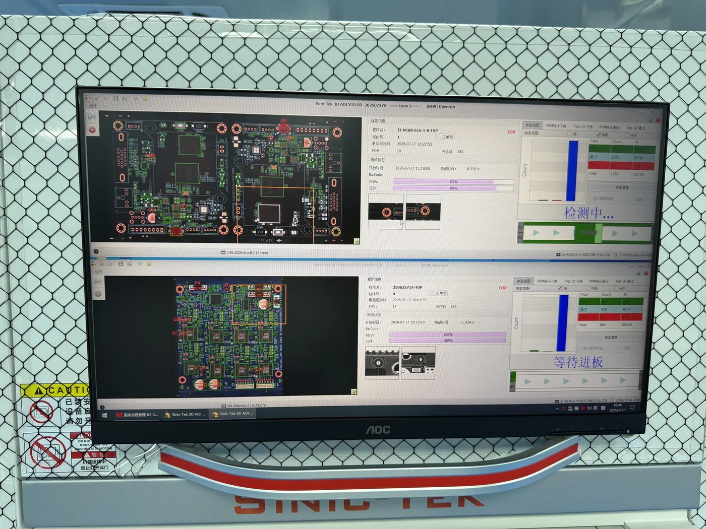
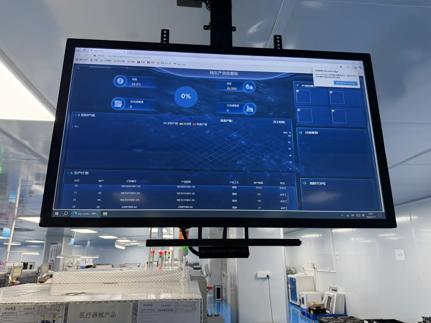
9× 3D SPI and 5× 3D AOI stations — the AI-assisted Sinic-Tek A510D AOI is linked live to MES — with X-Ray (UNICOMP AX8200) for hidden BGA and QFN joints, plus ICT/FCT. Coplanarity is measured on-line to ±0.03 mm per lead.
Deionized-water cleaning
Assemblies are cleaned with deionized water where the process calls for it, verified by 60–80× microscope inspection against the acceptance standard.