
柔性PCB制造商
超过20年的信赖之选
ISO 9001|ISO 13485|IATF 16949
深受行业领先企业信赖


获取即时报价
上传您的Gerber文件,获取即时DFM分析和优惠价格。
99%
准时交付率
2,500+
活跃客户数
15年+
行业经验
1-50
层数范围
技术能力
专注于 柔性工程
我们的工艺专为应对柔性电路的独特几何挑战而设计,从动态弯曲到紧密折叠。
应用领域
我们的电路赋能各行各业

医疗设备
为植入设备、监护仪和手术机器人提供可靠的柔性电路。

航空航天与国防
符合MIL-SPEC标准的高可靠性刚柔结合电路板。

汽车电子
用于传感器、车载娱乐系统和ECU连接的耐用PCB。

消费电子
适用于可穿戴设备和移动设备的紧凑型可折叠电路。
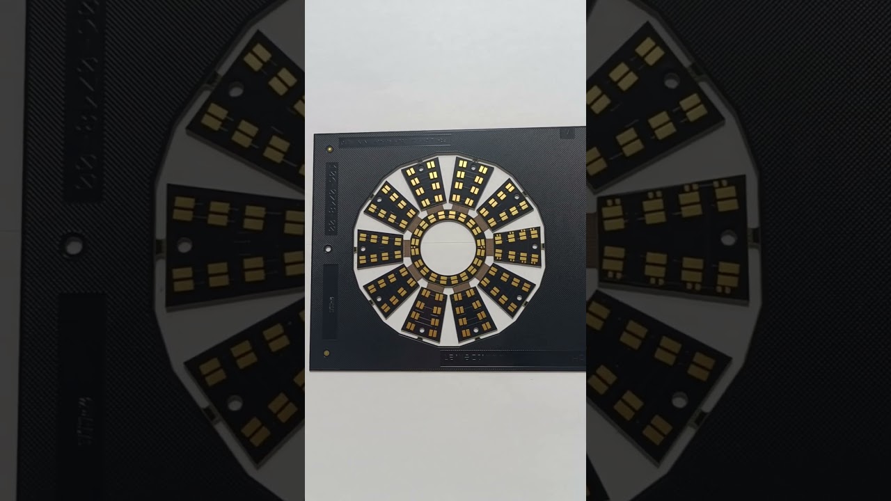
行业应用展示
查看我们为各行业设计的刚柔结合PCB产品
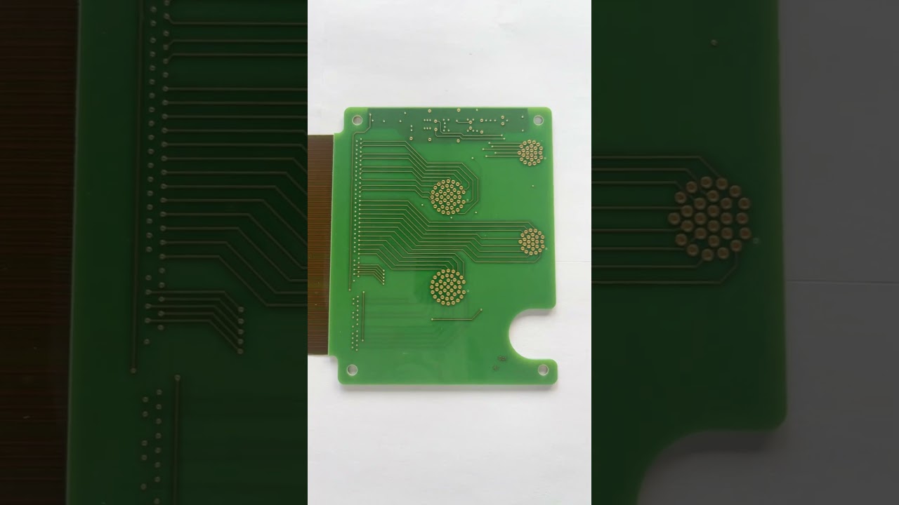
消费电子刚柔结合PCB
适用于消费电子设备的紧凑型刚柔结合解决方案
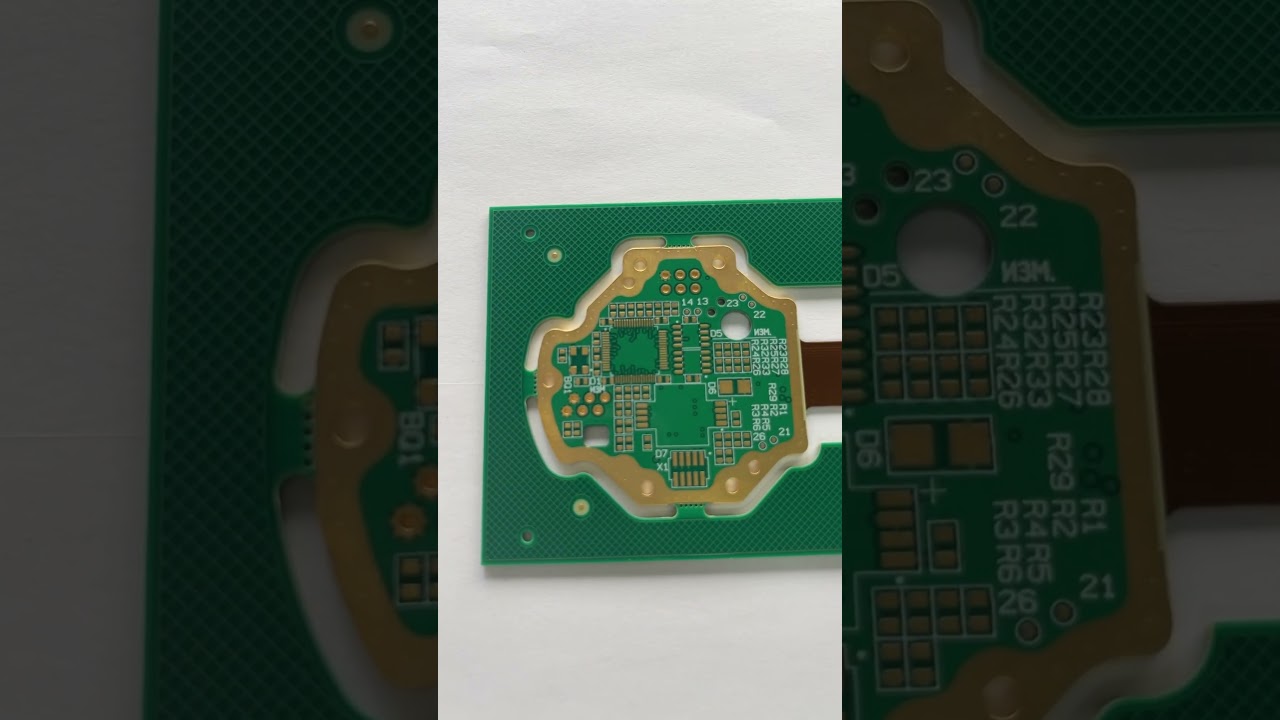
4层工业控制刚柔结合板
适用于工业自动化系统的高可靠性刚柔结合板
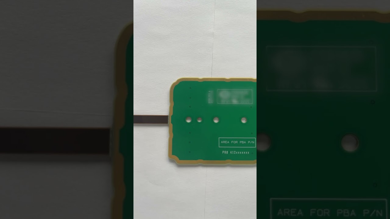
医疗设备刚柔结合PCB
为医疗设备应用定制的刚柔结合解决方案
消费电子刚柔结合PCB
适用于便携式消费产品的先进刚柔结合设计
为什么选择FlexiPCB满足您的柔性电路需求?
FlexiPCB是柔性印刷电路板(柔性PCB)和刚柔结合PCB的领先制造商,为全球客户提供高品质、精密工程的解决方案。我们先进的制造设施将尖端技术与数十年的专业经验相结合,交付满足最严苛规格的柔性电路。
我们专注于广泛的柔性PCB应用,从单层柔性电路到复杂的多层刚柔结合组件。我们的能力包括HDI技术、阻抗控制以及各种表面处理,包括化镍金、OSP和硬金电镀。

凭借ISO 9001:2015、ISO 13485(医疗)和IATF 16949(汽车)认证,我们确保所有产品的一致品质。我们对卓越的承诺使我们成为医疗设备、航空航天、汽车和消费电子等行业值得信赖的合作伙伴。
常见问题