
Fractured and cracked boards are some flexible PCB issues that many designers face now and then.
Because as much as they’re versatile with their ability to bend and twist to fit a user’s application, they’re not immune to errors.
This article discusses some common errors you’ll likely encounter when designing flexible PCBs and how to avoid them.
Table of Contents
- Why Flexible PCB Issues Occur
- 5 Common Flexible PCB Issues
- How to Avoid Flexible PCB Issues
- FAQs
- Conclusion
Why Flexible PCB Issues Occur
Flexible PCBs differ greatly from rigid boards. And a most common cause of flexible circuit errors is when designers build these boards using the same principles they employ in designing rigid boards.
Yet, flexible PCBs require flex-friendly design.
Also, you’ll often find no communication with the supplier when issues occur.
So it’s essential to consult your supplier and follow their recommendations keenly.
5 Common Flexible PCB Issues
The following are some issues designers face when designing flexible circuits.
Not Enough Spacing Between Solder Pads
In a flexible PCB, the solder mask or overlay openings are larger.
Therefore, there’s a risk of not leaving enough space between the conductor traces and the solder pads, resulting in short-circuiting.
To avoid short circuits in the solder bridges between connector pads, ensure sufficient room between each and the conductive trace next to it.
That way, it can accommodate the larger coverlay openings.
Coverlay Not Wide Enough
During fabrication, processes like copper plating and etching effect changes in the shape of a flexible PCB.
And if you’re used to designing rigid boards, it’s easy to forget to factor in processes like applying coverlay, stiffeners, die-cutting, and lamination.
So, to avoid issues, ensure to allow large tolerances for these processes by making the openings in the coverlay wide enough to make up for the shortcomings.
Stacked Traces
When designing flexible circuits, it’s vital that the copper stays on the axis of the bend, not stacked up on each other.
Otherwise, when flexing the circuit, you risk cracking the traces outside the bend radius.
And the further the copper traces are from the bend radius, the higher the risk.
Stress Points
Generally, creating stress points in flexible PCBs is daunting.
Because although trace arrangements work well for rigid PCBs, they’re unsuitable for flexible circuits.
See, wherever there’s a stress point when the area gets stretched, it often fractures or delaminates.
Solder Joints Too Close
Usually, the solder joint is more rigid than the rest of the copper trace to which the solder is bound. While this is not an issue with rigid PCBs, it is dangerous in flexible circuits.
See, a flexible circuit undergoes bending.
So if the joint is too close to where you’ll flex the substrate, the solder pad will crack, or the lamination will loosen.
To avoid this, be careful when joining the components not to affect the flexibility or functionality.
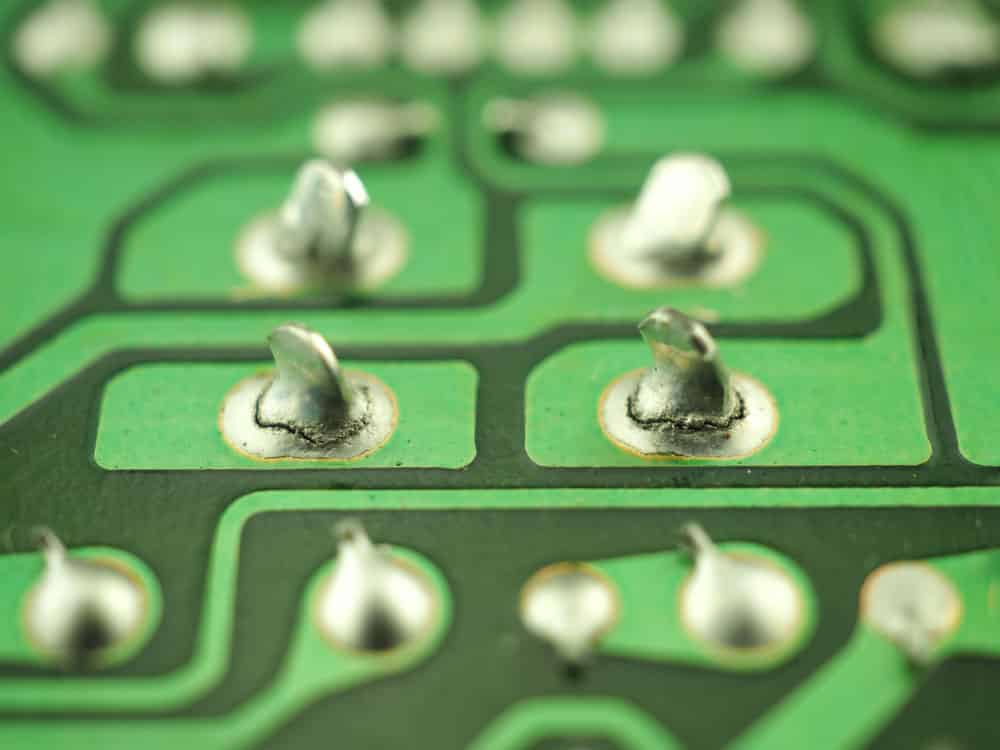
(Caption; Cracked solder joints)
How to Avoid Flexible PCB Issues
The best way to counter FCB errors is to consider the following factors in the design and production process:
Flexibility and Bend Radius

(Caption: a flexible bent circuit)
The copper will stretch and crack if a flexible circuit gets bent more than the design allows.
Therefore, it’s advisable to calculate the bend radius, the minimum radius to bend a flex circuit without causing damage.
To limit errors in the bend areas, do the following:
- First, you want to measure the bend radius from the bend’s inner surface, not outside.
- Also, avoid using plated through-holes within the bend areas
- And because conductors tolerate compression much better than flexing, make them 10 mils or smaller and place them inside the neutral bend axis.
- Further, avoid tight bends, as the tighter the bend, the more damage.
Remember the thickness of a flexible PCB and the materials used significantly impact the bend radius.
The IPC provides some design standards for minimum bend radius when designing flexible circuits in the IPC-2223 guidelines.
These include:
- Single layer flex thickness multiplied by 6
- Double layer: flex thickness multiplied by 12
- 3 layer: flex thickness multiplied by 15 to 20
- 4 layer: flex thickness multiplied by 24 to 30
- 5 layer: flex thickness multiplied by 34 to 40, and so on.
However, in dynamic bend applications, the layer count does not go beyond two (one-layer or two-layer).
And to measure the bend radius, you’ll multiply the flex thickness by 100.
Circuitry Layout
Interestingly, the circuitry layout determines the flexible PCB performance and longevity.
To that end, the following are some factors to consider to limit errors:
- First, never route signals at sharp angles.
- Second, to avoid an i-beam effect, don’t stack conductors. Doing so would reduce flexibility and increase stress and compression induced by flexing or bending, resulting in cracking.
- Further, stagger traces on the front and back when designing flexible multilayer circuits. Also, regarding traces, opt for curved ones, not those with corners.
Trace Width
At the point where the pad connects to the traces, thin it out.
That’s because this area (where the trace binds to the pad) is weak and can give in with time, causing the flexible circuit to fail.
Additionally, IPC-2223 standards also recommend supporting component areas with rigidizing stiffeners.
That way, there’s no binding in these component areas, eliminating cracking and other solder joint-related reliability issues.
Support for Pads
Provide mechanical support for the exposed copper in flexible PCBs by adding up to 1.5 mils of through-hole plating.
That’s because, due to the bending typical of flexible circuits, the copper on these boards can easily detach from the substrate.
Note, though, that non-plated through-holes and SMT pads require even more measures to ensure detachment of the copper does not occur.
Mechanical Stress Reduction
When there’s concentrated mechanical stress, such as in a design where a flexed area changes direction, radiused corners (rounded) are essential.
In addition, these rounded corners should have a relaxed radius.
Thus, avoid 90-degree corners; instead of 45-degree corners, use radiused ones.
Further, avoid the start/stop overlays and stiffeners simultaneously.
Otherwise, it alters the thickness, resulting in a mechanical stress concentration area.
FAQs
How do you test a flex PCB?
Thankfully, there are several tests you can perform, depending on the board’s application, including a board test, bend test, X-Ray, ACI, RCSE, ICT, and TDR.
What are the characteristics of flexible PCB?
Due to the polyamide they comprise, flexible PCBs are flexible, and you can bend or twist them.
In addition, they are lightweight, very thin, and have a high wiring density.
What are the disadvantages of flex PCBs?
Unfortunately, flex PCBs are more prone to design errors, especially if the user has more experience with rigid boards.
Additionally, they’re more vulnerable to damage during handling and, in certain applications, cost more.
Conclusion
That’s it. Now you know the kind of flex PCB issues you’re likely to encounter when designing flexible circuits and how you can avoid making these errors in the first place.
Just remember that although some of the functions of flexible PCBs are similar to standard PCBs, there’s a stark distinction between the two boards.
Therefore, designing flexible PCBs requires applying flexi-friendly principles to minimize errors.
We hope you find this article helps you design for success.