
Flexible PCB board shielding is an ever-growing and one of the most reliable techniques being adopted in the industry.
To begin with, we understand that flexible PCBs are very sensitive to emitting or absorbing either radio or electromagnetic interference.
And if you leave such interference unattended, it could negatively affect PCB performance and, in the worst cases, cause permanent damage.
Therefore, the solution is to adopt shielding mechanisms to prevent your flexible circuit board from radiating or absorbing EMI and radio frequencies. But how do you do this?
Worry not, as this article will address everything associated with flexible PCB board shielding.
Let’s get rolling.
Table of Contents
- Explaining Flexible PCB Shielding
- Types of Flexible PCB Shielding Materials
- EMC/EMI Shielding in Flexible PCB
- Flex PCB Shielding Considerations
- Design Tips To Avoid RF and EMI Interference
- FAQs
- Final Remarks
Explaining Flexible PCB Shielding
Most circuit boards are affected by electromagnetic (EMI) and radio frequency (RF) interference.
In short, EMI is a disturbance from an electrical source influencing the circuit board with conduction, electrostatic coupling, and electromagnetic induction.
Therefore, it reduces flexible PCB performance or even permanently disables its functioning.
And this is where flexible PCB shielding (EMI and RF shielding) comes in handy.
This involves methods to prevent RF and EMI interference from external signals.
Also, it prevents high-frequency signal leakage from affecting the surrounding circuits.
We usually use metallic barriers that can absorb RF and electromagnetic interference.
Below are some shielding applications in the military, communications, and medical fields.
- Medical systems: Patient monitoring systems, infusion pumps, and MRIs.
- Communication systems: RF communications and cellphones.
- Military systems: Communication, radar, and high-speed data transmission systems.
Types of Flexible PCB Shielding Materials
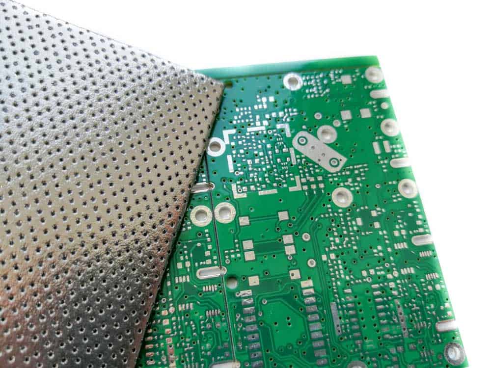
(Special purpose electronic PCB shielding material)
You must select a shielding material depending on the impact on mechanical bend capabilities, suitability for impedance-controlled designs, and shielding performance.
Generally, flexible PCB shielding happens using three material types.
- Specialized shielding films
- Silver ink
- Copper layers
Copper Layers
This approach involves using solid or cross-hatched copper layer planes, and you link them to the ground using stitched vias.
In this case, you sandwich the signal layer between the shield layers.
Many manufacturers also employ this approach in rigid circuit boards.
Additionally, you use solid copper layers to achieve a high degree of shielding.
However, cross-hatched copper layers come in handy when you don’t want to affect circuit board flexibility.
And although this method shields against EMI and RF interference, it raises the flexible board thickness and consequently increases the design cost.
Moreover, the extra PCB thickness might affect the board’s flexibility, thus affecting performance.
Furthermore, since you connect the shielding layers to the ground plane using vias, it affects performance because of the availability of vias in bending areas.
Remember, the IPC 2223 design standard prohibits vias in the bending sections since they reduce flexibility.
Silver Ink
Silver ink provides more circuit board flexibility and lower cost than copper shielding.
And although it’s more flexible, this option still requires an extra coverlay to preserve and encase the silver ink.
A flexible PCB with silver ink is usually about 75% thicker than a non-shielded option.
With silver ink, you apply selected perforations in the PCB main overlay.
Therefore, the perforations will expose the ground planes and give room for electrical connections.
As a result, the silver ink will flow through the holes to create a connection between the signal layer and the shield.
Generally, silver ink reduces the number of manufacturing steps and material layers.
However, this option is not feasible for impedance-controlled designs.
Specialized Shielding Films
These are the most common shielding options, allowing for the smallest structures.
Also, they’re perfect for dynamic bend applications, providing effective performance.
In the specialized shielding film arrangement, you laminate an exterior insulating layer, electrically conductive adhesive, and metallic deposition layer.
Next, you use pressure and heat to bond the laminate on the coverlay surface.
Moreover, you connect the ground circuit in the same way as the silver ink option above.
As a result, the conductive glue will electrically link and bind through the coverlay selective holes.
This method offers the smallest thickness impact of the other two options.
Therefore, the shielded film thickness is only about 15% to 20% of a non-shielded film.
However, specialized shielding films aren’t perfect for controlled impedance designs since they increase the tolerance value.
EMC/EMI Shielding in Flexible PCB
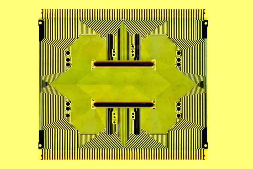
(A complete flexible circuit board)
Designing a flexible circuit board is both a mechanical and electrical task.
Therefore, there is a need to balance these two parameters to guarantee effective performance.
However, sometimes a problem of electromagnetic interference or radio frequency interference arises in the circuit board.
Applying suitable shielding mechanisms helps to prevent the flexible PCB from radiating and absorbing EMI.
Follow the steps below to bond a shielding film on your flexible circuit board.
- First, cust the EMI as per the dimensional requirement
- Secondly, remove the protection found at the bottom
- Thirdly, stack the film at the appropriate location on your circuit board
- Finally, laminate the layer using heat and pressure
Flex PCB Shielding Considerations
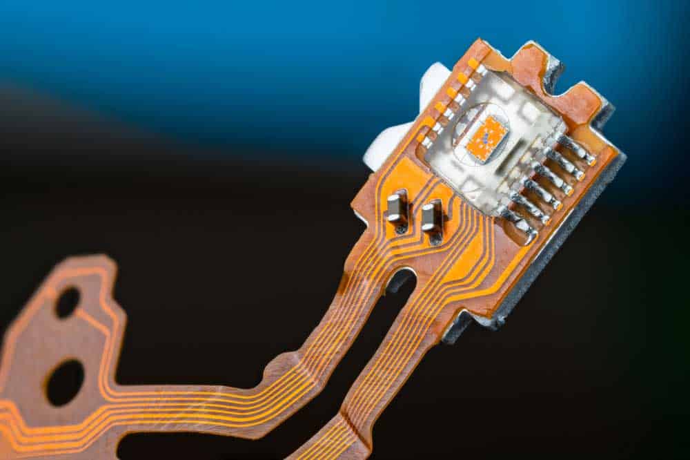
(An optical sensor on electronic PCB)
There are two primary considerations when selecting your EMI shielding options: Controlled impedance and bend requirement. Let’s discuss them in depth below.
Bend Requirements
Every shielding method you select adds a certain thickness to the board.
And since the PCB minimum bend capacity is a thickness function, it’s likely to limit PCB flexibility.
Therefore, you should accurately establish the bend type and minimum bend radius requirement during the material selection and PCB design process.
Additionally, it would be best to consider whether you want to design a static or dynamic PCB.
Generally, a dynamic PCB has a higher bending capacity than a static option.
Controlled Impedance
The controlled impedance signal requirement also restricts the shielding method you choose.
Therefore, to obtain proper impedance values, ensure the shield contains electrical properties that meet the electromagnetic interference and reference plane criteria.
Design Tips To Avoid RF and EMI Interference
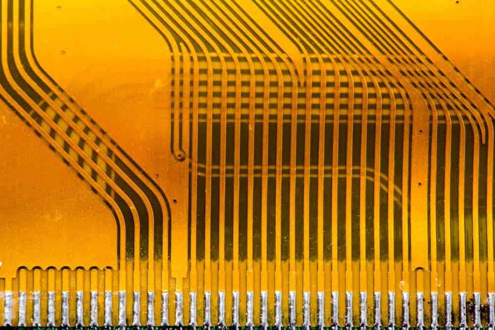
(A flat ribbon cable)
Consider the following tips to prevent RF and EMI interference:
- Employ the ground plane to prevent RF and EMI interference. The ground plane has a single power supply terminal and the PCB power return path.
- Keep the PCB return paths short.
- Never use traces having sharp angles since they cause signal and impedance fluctuations.
- Don’t place vias on your circuit board in differential pairs.
- Remember to pull back the ground and power planes from the PCB edge.
- Connect bypass and decoupling connectors to your PCB ground plane.
- Separate the signal traces to eliminate coupling cases.
FAQs
How do ferrite beads limit EMI interference?
Ferrite beads are designed with a core having a magnetic field attracted to the electrode’s magnetic field.
Therefore, the core prevents EMI by absorbing high-frequency noise and blocking low-frequency noise.
Does PCB board shielding improve performance?
Circuit board shielding helps to protect the board against absorbed and radiated electromagnetic interference.
Generally, EMI reduces the effective performance of a PCB.
Therefore, shielding will improve signal integrity and increase reliability.
Which layer is used for the protection of flexible PCB?
Flexible circuit boards are designed with delicate materials like copper, which can oxidize when exposed to air.
Therefore, you must cover the materials to protect them from external effects.
We refer to the layer we use to cover flexible PCBs as coverlay or overlay.
And in most cases, the coverlay consists of solid polyimide sheets with a flexible adhesive layer.
Final Remarks
It’s common knowledge that flexible PCBs are sensitive to absorbing or emitting RF and EMI interference.
Such occurrences affect the circuit board performance and, in the worst cases, cause permanent damage.
Therefore, we recommend applying PCB shielding mechanisms to limit the EMI radiation and absorption.
All the information we have provided above is a good starting point for achieving this.
Should you need further clarification, we are always available to help.