
A bare flex PCB is an important part of the printed circuit board manufacturing process.
At the bare stage, you can conduct tests before finally deciding to start mounting components.
However, since the bare flexible PCB is the foundation of circuit board manufacturing, you must understand how to make one.
Luckily, we’ll detail everything you need to know before starting your project on flexible printed circuit boards. Let’s get started.
Table of Contents
- What Is A Bare Flex PCB?
- Bare Flex PCB Manufacturing
- Testing Bare Flex PCBs
- Bare Flex PCB Testing Benefits
- Bare Flex PCB Pricelist
- FAQs
- Conclusion
What Is A Bare Flex PCB?
A bare flex PCB is the base of the printed circuit board assemblies.
In other words, they lack any through-holes or electronic components but conductive pathways only.
When manufacturers manufacture bare flex PCBs, they determine the substrates, solder masks, and conductive pathways.
Afterward, they add components and the necessary through holes for the bare flex PCBs to function as you require.
A bare flex printed circuit board also differs from a PCB assembly (PCBA).
It is only after the addition of components like resistors and capacitors that the bare PCB becomes a PCBA.
And manufacturers prefer to start with bare PCBs as they are easier to test to ensure the suitability of the circuit boards to their purpose.
Bare Flex PCB Manufacturing
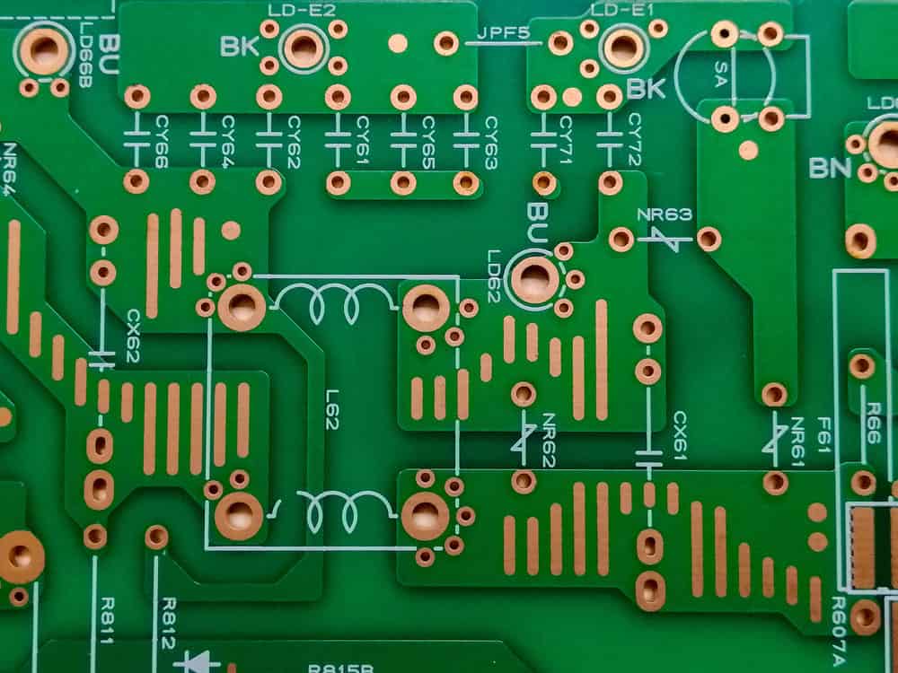
(A bare flexible PCB)
As the section above shows, manufacturers test the bare flex PCBs to ensure everything is in order before assembly.
They must ensure that the manufacturing process meets industry standards and regulations.
However, the success rate diminishes when they fail to adhere to the right manufacturing processes and use of proper materials that include:
- FR-4: It is a flame-retardant material that manufacturers commonly use as a base material for printed circuit boards. It gets its name from its flame-retardant properties coupled with epoxy resin.
- PTFE: Polytetrafluoroethylene or Teflon is another material manufacturers use as a PCB laminate material. Moreover, it has excellent dielectric properties than the FR-4.
- Metal: Depending on the application, bare flex PCB manufacturers use certain metals like aluminum and copper to form conductive pathways. Another less popular metal is iron which improves the structural integrity of the boards.
Steps
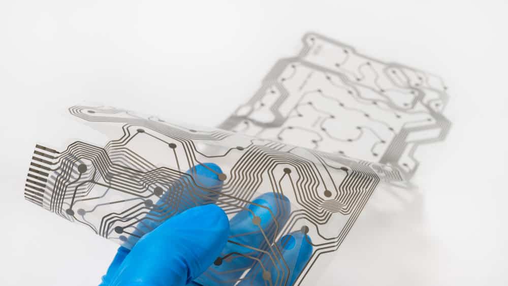
(Holding a bare flex PCB with conductive paths)
Now that we know the materials let’s look at the steps you’ll take to manufacture your bare flex PCB.
- First, start by drilling holes for the vias. It is time-consuming since one must ensure the holes are precise. Additionally, you do so to avoid massive losses since you will have to fabricate a new bare PCB.
- Second, pass the drilled bare PCB through a hole metallization process. With this step, the holes coat with a thin layer of carbon that also acts as the cathode.
- Thirdly, laminate the bare flex PCB with photosensitive film material to make imaging possible. Afterward, pass the laminated board through a direct imaging machine for imaging.
- Fourth, a periodic pulsed plating method is used to plate the bare flex PCB. Additionally, ensure you use the correct amount of copper metal for each conductive pathway on the board.
- Fifth, etch the bare flex PCB to remove the excess copper from the circuit. The process is important as the unwanted copper traces may lead to short circuits. Interestingly, all you need to do is to dip the bare circuit board into an etching chemical solution containing ferric chloride. And be careful, as you can easily under-etch or over-etch your bare flex PCB.
- Sixth, apply a solder mask on either side of your flex PCB. A solder mask is essential as it protects the copper traces from damage. Furthermore, it prevents the copper traces from short-circuiting or disconnecting.
Screen Printing, Surface Finish, and Inspection
Once you’re done applying the solder mask, here are additional steps.
- Seventh, apply ink on the mesh screen in a process called screen printing. It is a crucial step as it aids in detailing logos and markings on the board.
- Eighth, apply a surface finish like HASL, silver, and copper on the PCB’s copper pads. Interestingly, the surface finish must be of a certain thickness so that the bare PCB remains functional. You can determine its thickness with the use of an X-ray fluorescence instrument.
- Finally, inspect your bare flex PCB for any correctional defects. Sometimes, defects like poorly drilled holes render your board useless, and you may have to manufacture another one.
Testing Bare Flex PCBs
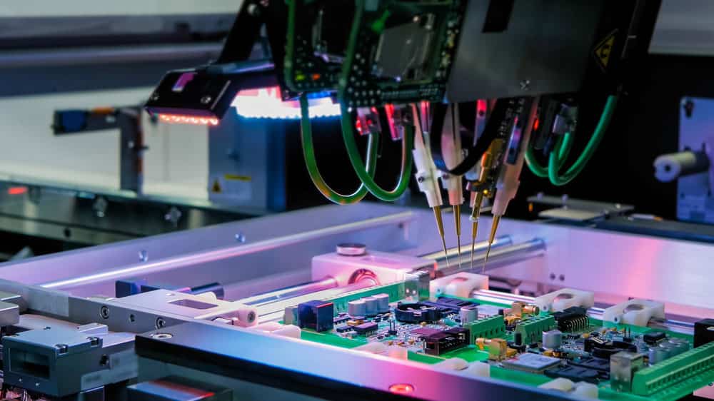
(A flying probe test at a PCB manufacturing plant)
Like any manufacturing process, some errors will likely happen when manufacturing bare flex PCBs.
For instance, you may have applied too much copper, which may lead to corrosion.
Conversely, you may find that the copper traces are too thin that they can lead to short circuits.
Luckily, you can test your bare flex PCB to identify these faults.
In this section, let’s look at two standard bare flex PCB testing types.
Flying Probe Test
It is one of the most common tests printed circuit board manufacturers use to test bare flex PCBs.
The test relies on robotic arms with poles with testers that verify all connections of the bare flex PCB.
Additionally, the robots rely on instructions from software specific to a particular board to test connections and inductance.
Also, the flying probe test checks capacitance and resistance.
Pinned Failure Test
The pinned failure test is the in-circuit method for testing large-scale bare flex PCBs.
It is a fast process that takes less than a minute to conclude while delivering accurate board analysis.
However, the testing method is costly as you have to restructure new pin arrays and fixtures to suit individual flex PCBs.
Bare Flex PCB Testing Benefits
As much as it may seem that bare flex PCB testing is not a vital step, in reality, it is a crucial step.
For instance, it is through testing that you identify insufficient or excess copper material in the conductive pathways.
Second, identifying problems before assembly will save you a lot of resources that you may incur if you fail to test the board.
For example, you may find the conductive pathways too thin to pass electric current when you’re past the assembly process.
Consequently, you will have to disassemble the board’s components.
This a time-consuming step, and you can avoid such with proper testing at the bare PCB stage.
Bare Flex PCB Pricelist
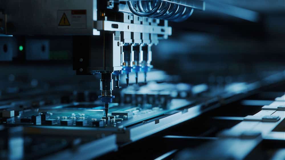
(Placing components onto a printed circuit board)
The prices of bare flexible PCBs vary significantly depending on their complexity and the materials used in manufacturing.
For example, a bare flex PCB for a robot will cost more than one for a calculator.
A higher price tag doesn’t necessarily translate to a better board.
Therefore, do thorough research before settling on a certain board, as cheap might be expensive too.
Surprisingly, some bare flex PCBs are as cheap as $1, while others cost more.
FAQs
When do you consider bare flex PCB testing?
Always consider bare flex PCBs testing to ensure your board functions properly.
Generally, it is through testing that you can identify faults that may hinder the regular operation of your board.
Furthermore, testing at the bare flex PCBs stage saves you time and money as you identify the errors early during manufacturing.
What’s the IPC standard for bare flex PCBs?
The IPC standard for bare flex PCBs falls within the 2220 series, among others.
For instance, the IPC 2221 addresses materials, design layout, and thermal management of your bare flex PCBs. Moreover, it addresses the board’s mechanical and physical properties.
Conclusion
You can manufacture a flex PCB with the right tools and expertise to suit your project.
Luckily, we’ve gone into detail to give you vital information to kick-start your journey into making bare flex PCBs.
And remember to test your bare PCB before assembling any components onto it, as it will save you a lot of resources.
Lastly, ensure that you abide by the industry standards and regulations to promote the safety and longevity of your PCB.