
Demand for the 8 Layer flexible PCB has significantly increased over the last few years.
After all, these boards offer many advantages, including unparalleled design flexibility, enhanced circuit density, and elimination of mechanical connectors.
Also, they have the unique ability to work with simple and complex electronic applications.
Read on to learn more about these flexible circuits.
Table of Contents
- What Is 8 Layer Flexible PCB
- Materials Used to Make 8-Layer Flexible PCBs
- 8 Layer Flexible PCB Stackup
- Tips for Building an 8-Layer Flexible PCB Stackup
- Advantages of 8-Layer Flexible PCBs
- 8 Layer Flexible PCB Application
- FAQs
- Conclusion
What Is 8 Layer Flexible PCB
As the name suggests, the 8 Layer flexible PCB is a multi-layered circuit board with eight layers.
Now four of these layers are signal layers, and the other four are planes, and they provide room for routing, which is necessary for applications that require multiple power islands.
Usually, the 8 Layer PCB gets installed in compact electronic pieces with very restrictive spacing requirements.
And this could be anything from laptops, motherboards, and wearables to communication backplanes.
Also, the board’s increased routing space with its additional two planes can enhance EMC performance.
Materials Used to Make 8-Layer Flexible PCBs
Conductive Materials
So the primary and most widely used material is copper.
The reason it’s used so much is it’s one of the most effective conductive materials.
See, it’s needed for the fabrication process to create the layer stackup.
For one, that’s primarily because it’s a good conductor of heat.
Thus, copper promotes proper signal transfers and minimizes heat accumulation on a component.
Also, it’s a more affordable alternative to other materials, such as gold or silver.
Substrates
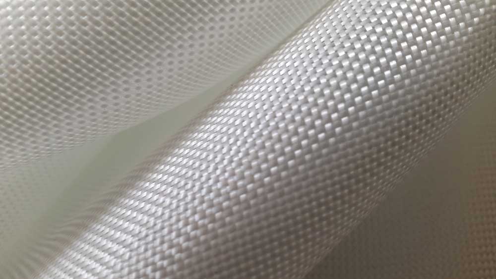
(Caption: Woven fiberglass material)
Most rigid PCBs you’ll find today use a base material of woven fiberglass fused in epoxy resin.
Undoubtedly, this base material is an actual fabric still considered rigid.
However, if you observe just one laminate layer, you will find that it has a fair amount of elasticity.
See, the cured epoxy resin causes the board to become rigid.
Also, using epoxy is why these boards often get referred to as organic PCBs, which are not flexible enough for most applications.
That said, if you want a simple assembly that won’t undergo constant movement, then this substrate will suffice.
On the other hand, polyimide is the most common substrate for a flex PCB substrate, including the 8 Layer PCB.
That’s because it’s highly flexible and robust and offers some of the best heat resistance features.
8 Layer Flexible PCB Stackup
Now the 8 Layer stackup comprises four plane layers and four signal layers.
As you would assume, these multilayer boards also tend to feature more than one conductive layer.
That means anyone working with such PCBs must clearly understand how a stackup functions.
First, the 8 Layer arrangement composition of conductive and insulating layers makes up a board.
In addition, a formidable 8 Layer stackup will assist you quite effectively when dealing with signal integrity issues.
It’s important to note that a ground or power plane separates one signal layer from another.
That way, it can reduce EMI emission and susceptibility.
The other thing is that a PCB designer must decide on the core material and prepreg the manufacturer should use during the board’s construction.
Now the choice of materials and their thickness can potentially affect impedance control.
And undoubtedly, this is an important element in the overall transmission line design.
Another vital factor you should ensure is that the PCB manufacturer can produce the 8 Layer stack-up specified.
Tips for Building an 8-Layer Flexible PCB Stackup
Get the Routing Right
In certain situations, an 8 Layer PCB stack-up may comprise up to six signal layers.
That means you must perpendicularly route the signal traces on the adjacent layers.
When you route them that way, you minimize issues of crosstalk.
To be on the safe side, you should always try to route signal layers differently based on subsequent layers, regardless of whether they’re separated by ground or power planes.
Align the Ground Plane
Usually, you should avoid splitting the ground plane, as this may lead to impedance discontinuity.
In addition, you need to ensure that the components on the outer layers possess low impedance.
To do that, you should connect these outer layers through vias that lead to the ground planes.
Short Return Path
Visualizing the return route/path associated with high-speed signals would be best.
And that’s regardless of whether or not these routes are on the inner layers.
Also, you should ensure that the path is short and, therefore, less likely to cause any interference with the other components.
Use the Vias
Completing a PCB stack-up design involves determining and routing the traces.
However, this process also includes determining copper weights, where to use the vias, and the kind of vias to implement.
When it comes to the specifications for your designs, you must work with your CM.
So ensure you consult with them when making these determinations since CMs usually avoid specific visa types such as the via-in-pads.
Advantages of 8-Layer Flexible PCBs
If you use the 8 Layer flexible PCB, here are some advantages you can expect:
- Reduce radiation: By being devices meant for high-speed applications, multilayer PCBs are by nature highly susceptible to radiation. However, when you use an 8 Layer flexible PCB, you reduce the radiation from electromagnetic interference.
- More Circuitry: The more layers a circuit board has, the more room for circuitry and wiring for complex applications requiring more components. Too many layers can compromise a board’s reliability and stability, so the 8 Layer is a good balance.
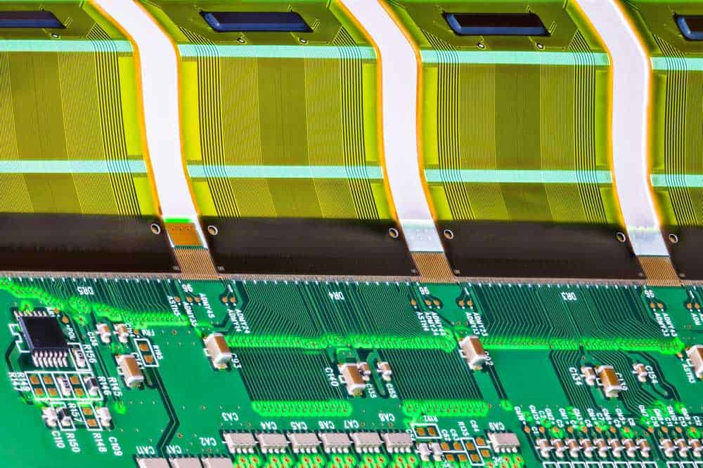
(Caption: Components on circuit board)
- Increased functionality: An 8 Layer is a reliable PCB that can function in various applications. For one, it has several layers of conductive material. This makes it a reliable PCB because the conductive material the layers comprise enhances signal traces.
- Lower operation costs: This multilayer PCB requires minimal cleaning.
- Also, you’ll seldom need to repair or replace it. That means these devices require a lower level of maintenance, which translates to reduced operating costs.
8 Layer Flexible PCB Application
Now this PCB has several applications, typically more complex ones. These include:
- Devices used in the aviation industry
- Medical devices
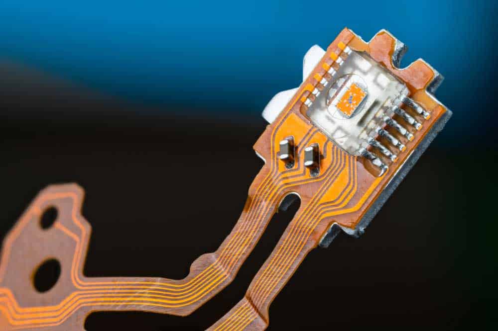
(Caption: Optical sensor applicable in optical heart rate monitors)
- Various electronic tools in the manufacturing industry
- Various equipment employed in the chemical processing industry
FAQs
How Thick is a Flexible Circuit?
The thickness varies from one flexible circuit to another depending on the copper thickness and the number of layers.
But generally, it ranges between 14 mils and 32 mils.
Usually, the 1 Layer and the 4 Layer flexible circuits measure 14 mils and 32 mils, respectively.
How Many Layers Can a Flex PCB Have?
The number of layers associated with a flex PCB will largely depend on the design specifications.
That’s the reason it’s not uncommon to hear of 12 layers.
Nonetheless, it’s important to remember that the greater the number of layers, the more difficult it is to stack them up.
Also, as mentioned earlier, too many layers compromise a board’s performance.
Is it Possible to Have an 8-layer Flexible PCB?
Yes, it is. See, an 8 Layer flexible circuit board can flex up to several million times.
That makes it ideal for circuit boards that have numerous moving components.
Conclusion
That’s it on the 8 Layer flexible PCB. Undoubtedly, this board is reliable and has several advantages.
For example, it offers increased functionality, more room for circuitry, and lower radiation at lower operational costs.
We hope you’re now better positioned to decide whether or not this PCB type suits your intended functionality.